
The discovery of the transistor effect in 1947 enabled microelectronics to develop very rapidly. Currently, it is found in various sectors such as automotive, computing, telecommunications, and even medicine. Furthermore, microelectronics and the software industry have contributed to numerous innovations.
Now that we are focusing on thin-film deposition techniques, it is essential to learn more about this subject. Discover what thin-film deposition is and its importance. Then, explore the different types of techniques and how they work. Next, examine the advantages and disadvantages of these thin-film depositions. Finally, consider how thin-film deposition is used in industry.
What is thin film deposition and why is it important?
Thin-film deposition can be defined as a set of processes aimed at depositing a thin layer or film onto a substrate surface. However, some techniques allow for the deposition of layers a few nanometers thicker. Thanks to thin-film deposition, it is possible to create many compounds that were previously impossible to produce. This compound fabrication process is found in:
- The field of optics when it comes to reflective or anti-reflective coatings
- The electronics sector through the implementation of layers of insulators, conductors or semiconductors for integrated circuits.
Types of thin film deposition techniques
Two main categories of thin film deposition techniques can be observed:
- On the one hand, the type of chemical deposition technique
- On the other hand, the physical thin-film deposition method
Chemical vapor deposition (CVD)
When a precursor fluid undergoes a chemical reaction, it leaves behind traces of solid layers. Because the fluid is deposited on a solid surface, the surface is completely covered. Here are some examples of chemical thin-film deposition:
- Coatings
- The sol-gel process
- Spin-coating
- Vapor deposition…
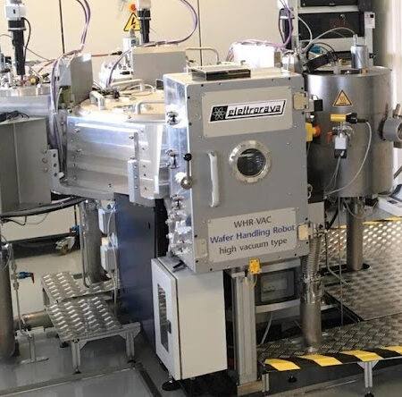
The physical thin-film deposition or PVD technique
This second category of thin-film deposition techniques includes mechanical, electromechanical, and even thermodynamic processes. Its objective is the production and deposition of a solid thin film. The substrate placed on top will extract energy from the particles contained within the material. Maintaining this system in a vacuum chamber is done for two reasons:
- First, to allow for faster movement of the particles
- Then, to limit the presence of atoms or molecules in the environment, there is either vacuum evaporation or cathodic sputtering.
How does each thin film deposition technique work?
A material is categorized as a thin film when its thickness ranges from atomic layers to microns. Each technique operates differently, so let’s explore their respective methods.
The operating mode via chemical thin-film deposition or CVD
Bringing a volatile compound from a material into contact with another gas is one of the main functions of chemical deposition. The interaction between the gas and the volatile compound will trigger a chemical reaction, subsequently creating a solid product. Various energy sources are used to activate the chemical reaction. You can therefore choose between:
- Thermal CVD uses the substrate temperature to initiate the chemical reaction. This temperature is achieved either by direct heating, induction heating, or thermal radiation.
- Organo-metallic CVD or OMCVD which allows the decomposition of various precursor compounds using a low temperature.
- The CVD laser (LCVD), which can be a continuous or pulsed beam, stimulates molecules. This process aims to increase the reactivity of gaseous species.
- Plasma-enhanced CVD (PECVD) and the gas phase are exposed to a high-frequency field. This exposure will cause the formation of chemically active species (ions and free radicals).
The operation of the physical deposition or PVD technique
The physical deposition or PVD technique takes into account three components:
- Steam production can be achieved through vacuum evaporation, sputtering, or arc welding. Vacuum evaporation involves applying extreme purity to the coatings using Joule heating, heat induction, ion bombardment, and other methods. Sputtering is achieved by ionizing the atmosphere by applying a sufficient electrical voltage to two electrodes. Arc welding, on the other hand, is obtained by eroding one or more cathodes using high-intensity electric arcs.
- The electrical state of the substrate can increase the relative density of thin film deposition. This increase is facilitated by atom sputtering, regardless of the vapor phase conversion method. It is even possible for the substrate to be completely free of impurities before vapor phase conversion is initiated.
- The nature of the gas in the medium greatly influences the formation of a suitable compound. This most often involves the deposition of oxide, carbide, or nitride layers. Introducing these types of layers into a reactive gas environment (oxygen, nitrogen, methane, etc.) offers a significant advantage.
Advantages and disadvantages of each technique
Each technique is different.
The CVD technique
Strengths:
- L’obtention d’une meilleure conformité des films grâce à la réactivité de la surface du substrat
- Improving control of the various compositions
- The possibility of having selective deposits under certain conditions
- Reducing production costs through significant processing capacity
Weaknesses:
- Unsuitable for milling due to the very high temperature used by CVD
- Le CVD est surpassé par le PVD en matière de revêtements céramiques et composites
- The high temperature of CVD can cause cracks in the coatings.
- The existence of residual stresses caused by intense heat during the cooling process
The PVD technique
Advantages:
- Wear resistance and good chemical stability
- Improving the bond between thin films and tool matrix materials
- The creation of the first generation of TIN coating which is multi-composite (TIC, TICN, ZrN…)
- The ability to offer good electrical conductivity and excellent resistance to reflection
Weaknesses:
- The need to resort to the use of annealing
- The use of sophisticated and expensive equipment
- Metal deposits cause the machine to get dirty.
- PVD does not allow the deposition of all materials
Applications of thin film deposition in industry
Vapor-phase thin-film deposition is applied in industry according to its properties. These properties can fall under the following categories:
- Mechanical engineering refers to resistance against erosion, abrasion, and friction.
- Optics, when it comes to the reflection, detection, and transmission of radiation.
- Electrical when it comes to conduction and insulation
- Physico-chemical when it comes to diffusion barriers, corrosion resistance or even catalysis.
Thin-film deposition applications in industry relate to the ALD (Atomic Layer Deposition) technique. This technique primarily involves building up the monolayer. This is achieved through the successive deposition of pulses of the metal precursor onto the substrate surface. The objective of this technique is to:
- Purge the reactor of all unreacted species after each thin film deposition.
- Dispose of any by-products that did not react during chemisorption
To achieve the desired thickness, this process can be repeated as many times as needed.
If you require state-of-the-art equipment for testing or thin-film deposition, don’t hesitate to contact MicroTest.