CVD/PE-CVD
CVD/PE-CVD
Related products
Presentation
CVD (Chemical Vapor Deposition) is a process used to produce high-performance, high-purity solid materials. The substrate is exposed to one or more gas-phase precursors, which react and/or decompose on the substrate surface to generate the desired deposit. Frequently, reaction by-products, themselves in the gas phase, are produced and evacuated by the gas flow that continuously passes through the reaction chamber.
CVD is widely used to deposit materials in various forms: monocrystalline, polycrystalline, amorphous, epitaxial. These materials include silicon, silica, silicon germanium, silicon carbides, diamond carbon, fibers, nanofibers, filaments, carbon nanotubes, tungsten, high electrical permittivity materials, etc.
Thermal chemical vapor deposition (CVD) uses high temperatures to deposit thin films by reacting gases with a substrate, ideal for materials like silicon and graphene.
Metal-organic CVD (MOCVD) creates high-purity films using metal-organic gases under moderate pressure.
Plasma-enhanced CVD (PECVD) uses plasma to deposit films at lower temperatures, while inductively coupled plasma CVD (ICP-CVD) allows deposition at even lower temperatures, suitable for sensitive substrates such as polymers.
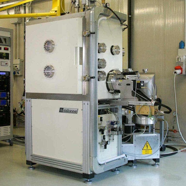
Our partner Elettrorava has been designing and manufacturing thin film deposition machines in Italy for over 35 years.
The equipment offered is flexible for R&D and production, and for multiple applications: optics, semiconductors, medical, photovoltaics, precision watchmaking, etc.
Specifications
LPCVD, MOCVD, PECVD, ICPCVD
- Base pressure HV: < 1x10⁻⁶ mbar
- Base pressure UHV: < 1x10⁻⁸ mbar
- Pumping system:
- Dry primary pump,
- high vacuum turbomolecular pump
- Sources:
- LPCVD: Resistive or infrared
- MOCVD: Heating power supply
- PECVD: DC, pulsed DC, RF, microwave
- ICPCVD: RF, microwave
- Additional sources:
- Optional plasma generator,
- Plasma generator
- Deposition area: Up to 12"
- Substrate handling:
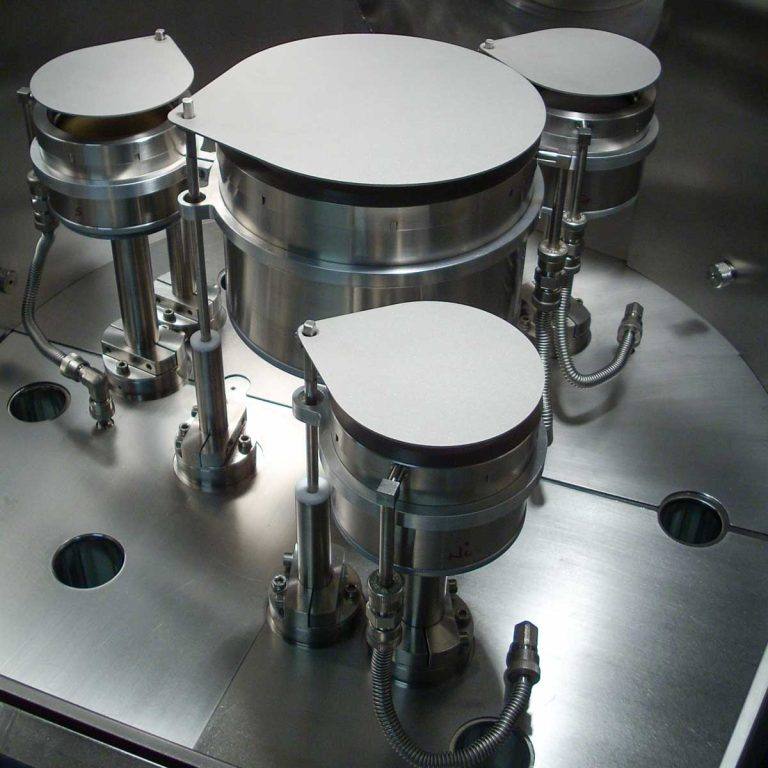
- Multi-wafer holder
- Rotation: up to 50 rpm
- Process temperature: Up to 1000°C
- Reactive process: One or more reactive gases (O2, H2, CH4, SiH4, etc.) and liquid precursors
- Thickness uniformity: Up to 3%
- Process control:
- LPCVD: Pyrometer or thermocouple for temperature control
- MOCVD: Optional optical monitor depending on deposited material type
- PECVD and ICPCVD: Multi-layer recipe control, optionally plasma control or ellipsometry.
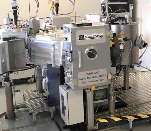
- Substrate load: Manual into main chamber or via load lock with manual or automatic manipulator
- Load lock: Single or multiple load locks, manual or motorized with multiple substrate holders
- Multi wafer loading: Optional multi-wafer cassette system up to 25 wafers
- Deposited materials: Metals, oxides, nitrides, carbides, semiconductors, carbon-based materials, organic materials
Strong points
• Single or multi-chamber (cluster)
• Up to 12 gas lines
• Solid, liquid or gaseous precursors
• Custom-made enclosures
• Simple automatic or manual loading or from a 5 or 25 wafer cassette
• Custom-made chuck
• Airlock possible
• Automatic pumping
• Multi-layer possibilities
• Doping possible
• Thickness measuring system (laser interferometer or quartz balance)
• Wafer up to 300 mm (more on request)
• Possible substrate temperature from +20° to +1000°C