Thermal evaporation and electron beam evaporation are two essential techniques for creating thin films. In thermal evaporation, materials like aluminum, gold, or silver are heated under high vacuum until they evaporate, forming a thin layer on the substrate. E-beam evaporation uses a focused electron beam to achieve the same result, allowing materials to be deposited at high temperatures at varying speeds, tailored to the desired properties of the film.
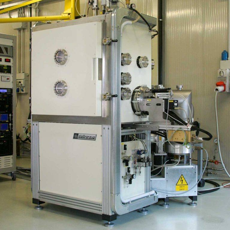
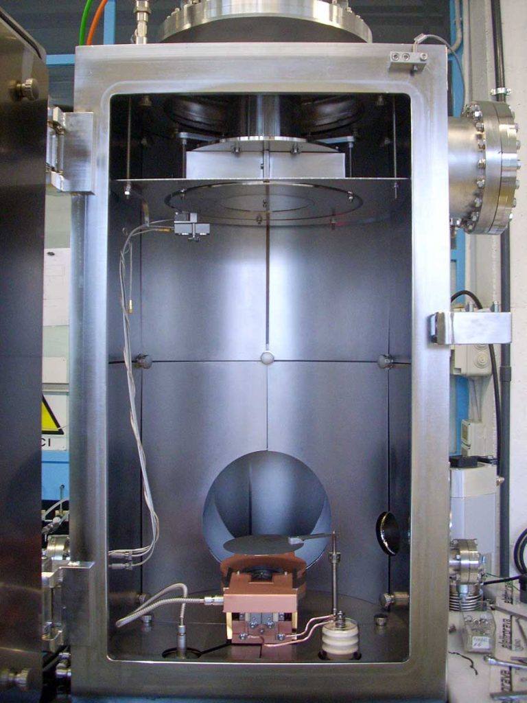
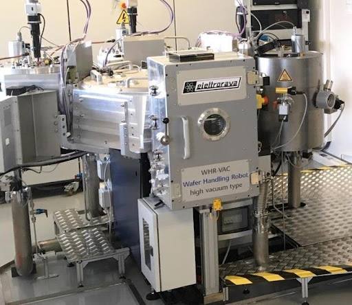
Our partner Elettrorava has been designing and manufacturing thin film deposition machines in Italy for over 35 years.
THERMAL EVAPORATION (PVD) - ELECTRON BEAM EVAPORATION (EBPVD)
- Base pressure HV : < 1x10⁻⁶ mbar
- Base pressure UHV : < 1x10⁻⁹ mbar
- Pumping system : Turbomolecular, Cryo, TSP
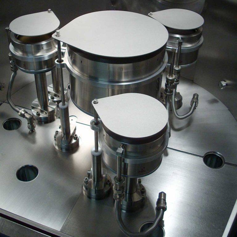
- Sources :
- PVD: Single or multiple coils, boats or crucibles
- EBPVD: Single or multiple electron beam with up to 8 crucibles, power up to 15 kW
- Additional sources : Electron beam, ion beam for etching/deposition, magnetron sputtering cathodes
- Deposition area : Up to 20”
- Substrate handling :
- Rotation : up to 50 rpm, optional planetary configuration
- Tilt: ±45°
- Offset (Z or X): up to 100 mm
- Process temperature : Up to 800°C
- Reactive process : One or more reactive gases (02, H2, N2, etc.)
- Thickness uniformity : Up to 3%
- Process control : Programmable quartz thickness controller and/or in situ optical monitor
- Substrate load : Manual in the main chamber or by load lock with manual or automatic joystick
- Load lock : Single or multiple load latches, can be motorized with multiple substrate holders
- Multi wafer loading : Optional multi-wafer loading system for up to 25 wafers
- Deposited materials : Metals, oxides, semiconductors, organics
- Particularly suitable for lift-off
- Custom speakers
- Plasma treatment, ion beam (stripping or assistance), oxidation or recrystallization possible
- Simple auto or manual loading or from 5 or 25 wafer cassette
- Custom Chuck (clamp hold or electrostatic hold)
- Static, dynamic, planetary, double planetary (satellite) and oscillating deposits
- Sas possible
- Substrate temperature possible from -60° to +1000°C
- Automatic pumping
- Multilayer possibilities with multi-crucibles
- Possible doping
- Thickness measurement system (laser interferometer or quartz balance)
- Wafer up to 300 mm (more on request)