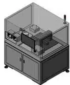
Designed for precision metrological inspection in the semiconductor industry, the wafer surface defect inspection machine enables automated high-resolution detection on 6", 8" and 12" wafers.
Thanks to a 12 MP industrial camera and motorized multi-zoom optics (5X to 100X), this solution is ideal for detailed analysis of post-manufacturing defects or final quality control.
It is perfectly suited for post-dicing, post-trimming or backend material entry inspection stages, with the ability to spot defects as small as 0.035 µm², including cracks, scratches, contamination or delamination.
Equipped with an intelligent interface and compatibility with MES (Manufacturing Execution System) systems, this machine integrates perfectly into automated or semi-automated production lines.
This inspection machine stands out for its operational modularity and high analytical accuracy:
Ideal for end-of-line inspection, post-packaging, or incoming quality control.