AOI: Automated Optical Inspection at the heart of semiconductor manufacturing
What is AOI?
In the semiconductor industry, the extreme miniaturization of devices imposes unparalleled quality control requirements.
L’Automated Optical Inspection (AOI) It is becoming an essential technology to guarantee the conformity of wafers, substrates and integrated circuits, by detecting defects invisible to the naked eye and ensuring the traceability of batches throughout the process.
Advanced AOI operation applied to semiconductors
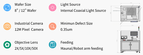
Modern AOI systems, such as those developed by Chernger Technologies, are based on an integrated architecture combining:
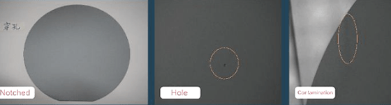
• High resolution optics : Industrial CMOS/CCD cameras capable of detecting micron-scale defects, essential for inspecting 200 mm/300 mm wafers and advanced substrates..
• Proprietary light sources : Chernger designs its own multi-wavelength LED modules, enabling multi-angle inspection and detection of surface defects (particles, scratches, organic/inorganic contamination).
• Proprietary algorithms : Intelligent detection based on AI and deep learning, for automatic recognition of complex defects (TTV, bow, warpage, micro-cracks, engraving defects, etc.).
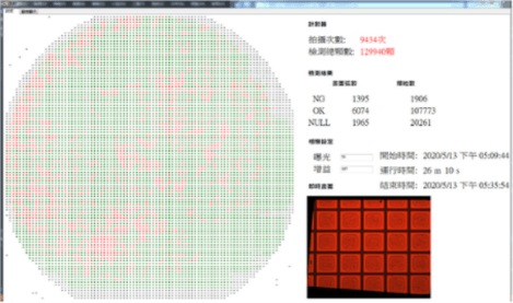
• Analysis and traceability software : Automatic generation of fault maps, SPC statistics, batch history management and integration with MES (Manufacturing Execution Systems).
Examples of specific applications
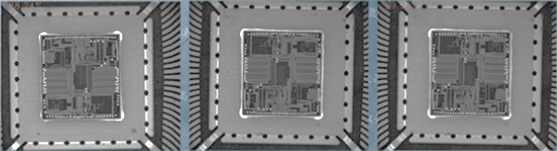
1. Inspection de wafers :
• Detection of particles and scratches on the active surface or backside.
• Flatness measurement (TTV, warp, bow): essential for lithography and assembly steps.
• Dimensional control of engraved patterns, verification of conformity to CAD masks.
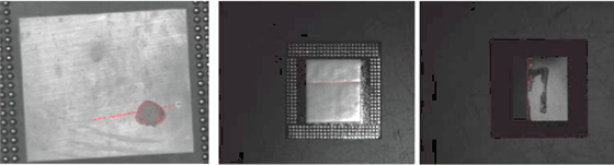
2. Substrate control and advanced packaging:
• Inspection of BGA, FC-BGA, CSP, PCB substrates for the detection of metallization, delamination or contamination defects.
• AOI on thin films and printed circuits on glass for MEMS, optoelectronics and sensor applications.
3. Inspection of the component carrier tapes:
• Automated multi-track control (up to 6 tracks, 24 m/min) for very high-speed IC packaging defect detection, with dynamic tolerance adaptation according to component type.
The advantages of Chernger solutions for semiconductors
• Vertical integration : Chernger controls the entire chain, from optical hardware to analysis software, guaranteeing rapid adaptation to market developments.
• Personalization: Tailor-made solutions depending on the wafer format, substrate type, nature of defects to be monitored, and production environment (cleanroom, inline, offline).
• Interoperability: Compatibility with industry standards (SECS/GEM, IPC, SEMI), facilitating integration into automated production lines.
AOI and continuous improvement
AOI Chernger systems do not just detect defects: they fuel a continuous improvement loop through statistical analysis, full traceability and real-time feedback to production equipment. This allows for a drastic reduction in the costs of non-quality, optimized yields and compliance with international certification requirements.
AOI, driven by Chernger Technologies’ innovation, is a pillar of advanced semiconductor manufacturing.
It enables the achievement of levels of quality and reliability essential for the electronics, automotive, optoelectronics and biotechnology markets.