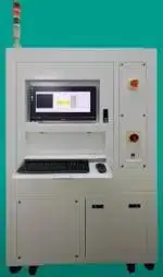
Designed to meet the stringent requirements of the semiconductor industry, the wafer surface particle inspection machine enables rapid and accurate detection of contaminants on glass or mirror wafers up to 12 inches.
Equipped with a high-resolution linear laser scanning system, it offers a detailed analysis of surface defects such as dust, polishing residues, or post-process particles.
Thanks to its ability to detect particles as small as 0.1 µm and to analyze up to 3000 particles with a statistical tolerance <±5%, this machine integrates perfectly into the quality control protocols of semiconductor substrates, including in cleanroom environments, up to ISO 6 depending on production needs.
- Inspection Technology: High-speed linear laser scanning
- Detectable Particle Size: ≥ 0.3 μm
- Supported Wafers: Up to 12 inches, mirror surface
- Accuracy & Repeatability: 1s < 0.3 μm
- Measurement Time: ≤ 60 seconds per wafer
- Additional Surface Analysis: Available in +2 minutes for complete mapping
- Particle Density Measurement: > 3,000 particles, tolerance < ±5%
- Adjustable refractive index: compatible with wafers and glass
- Data outputs: 3D particle distribution map, precise localization data
- KLA calibration: integrated cross-calibration mechanism
- Conversion of light scattering signals into particle size (logarithmic scale)
- Regionalization of measurements to targeted areas is possible
- Wafer support with specific characteristics (polished surface, thin film, etched)
- System compatible with standard calibration pellets
- 3D stereoscopic platform for topographic visualization of defects
- Automatic correction of values by comparison to standard references
- Integration possible with MES systems for traceability and quality reporting