MPI PA redefines excellence in photonic testing with its new product line inspired by the brightest constellations in the sky.
Our commitment to innovation is reflected in every aspect of their solutions,
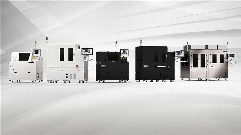
A complete range for all your needs :
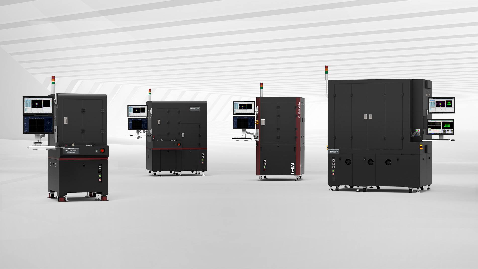
VEGA : Cutting-edge solutions for automotive lighting and backlighting (e.g. Laser Diodes)
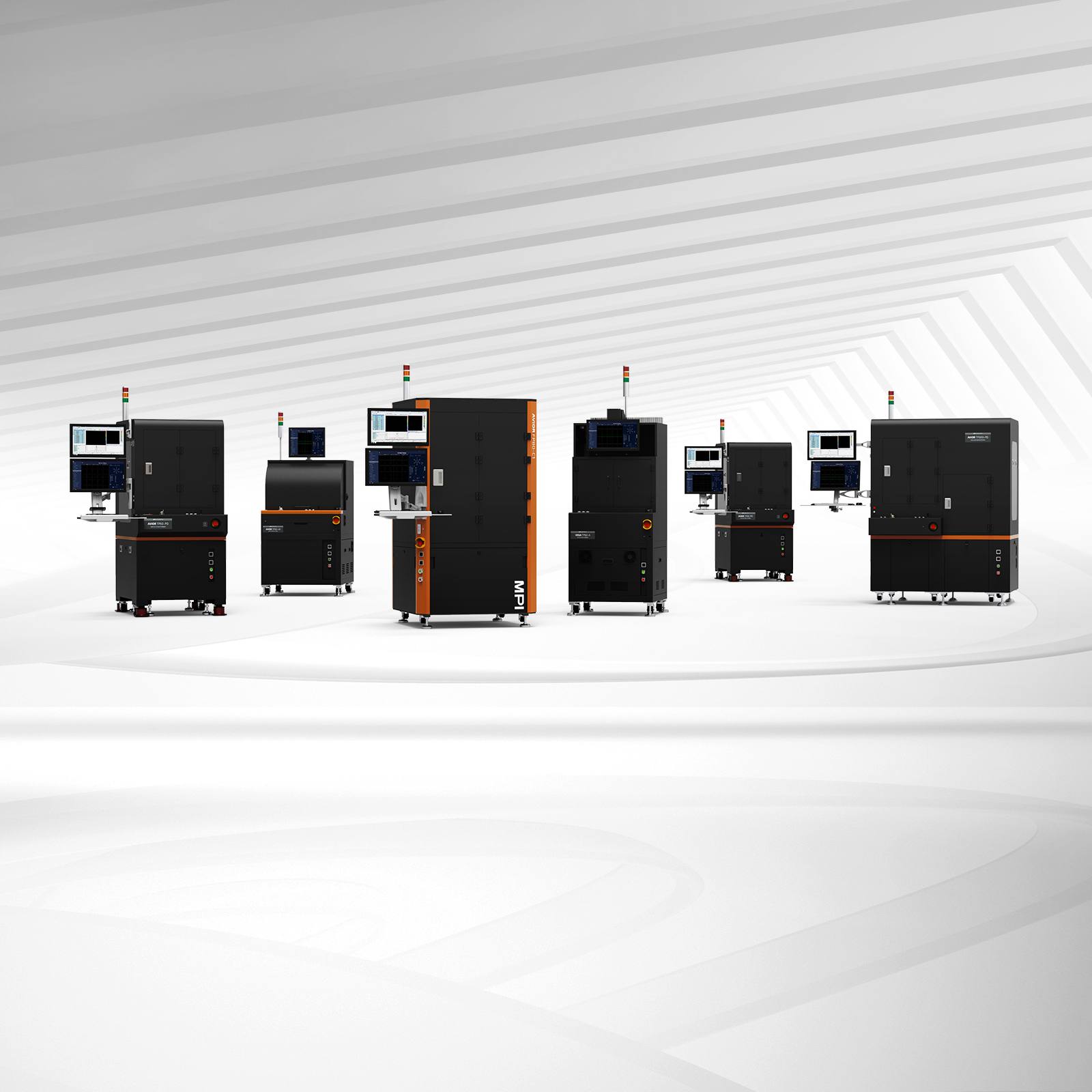
AVIOR : Precision testing for optoelectronic communication devices (e.g. Photo Detectors)
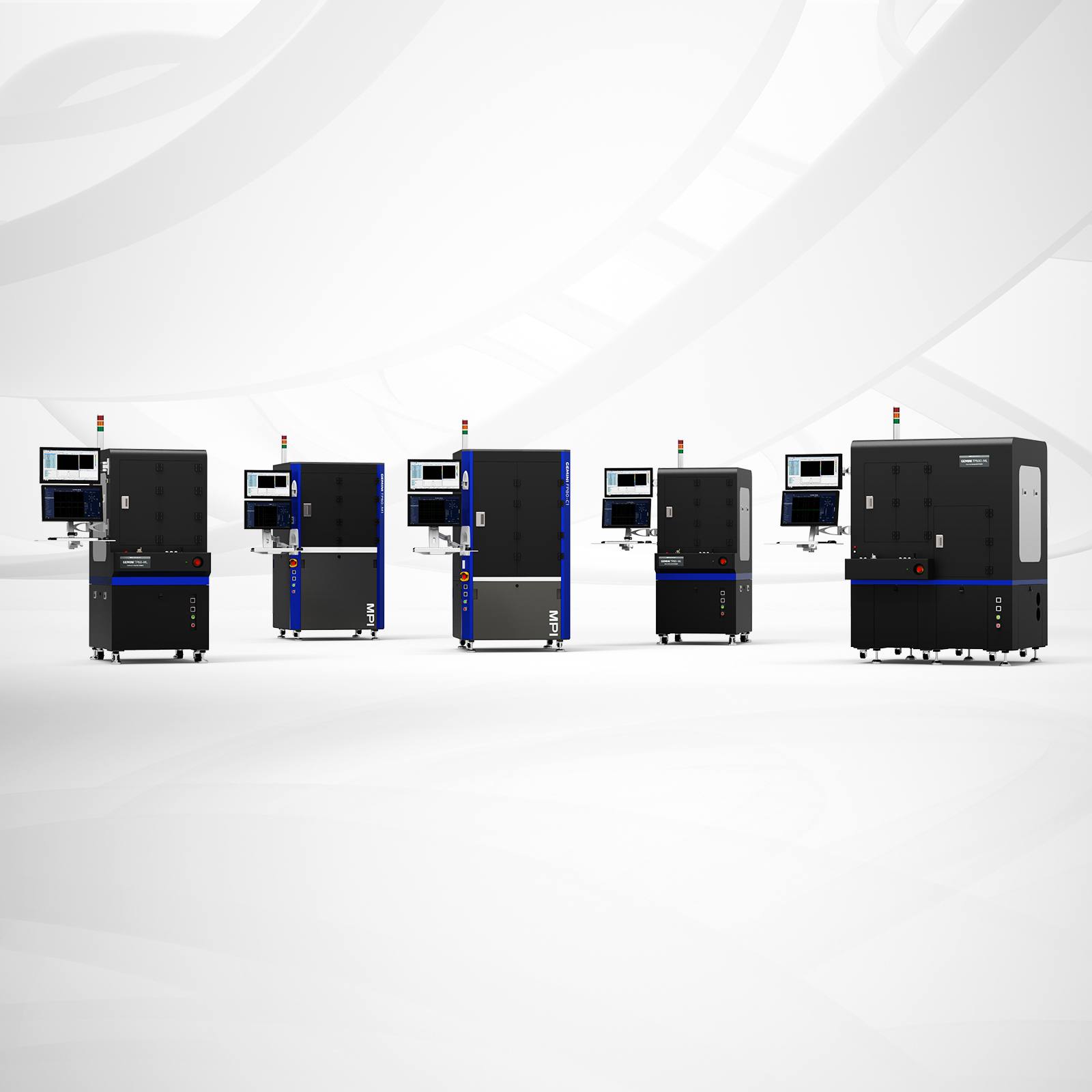
GEMINI : Advanced systems for micro display applications including wearables and AR/VR (e.g. Micro LED, Micro display)
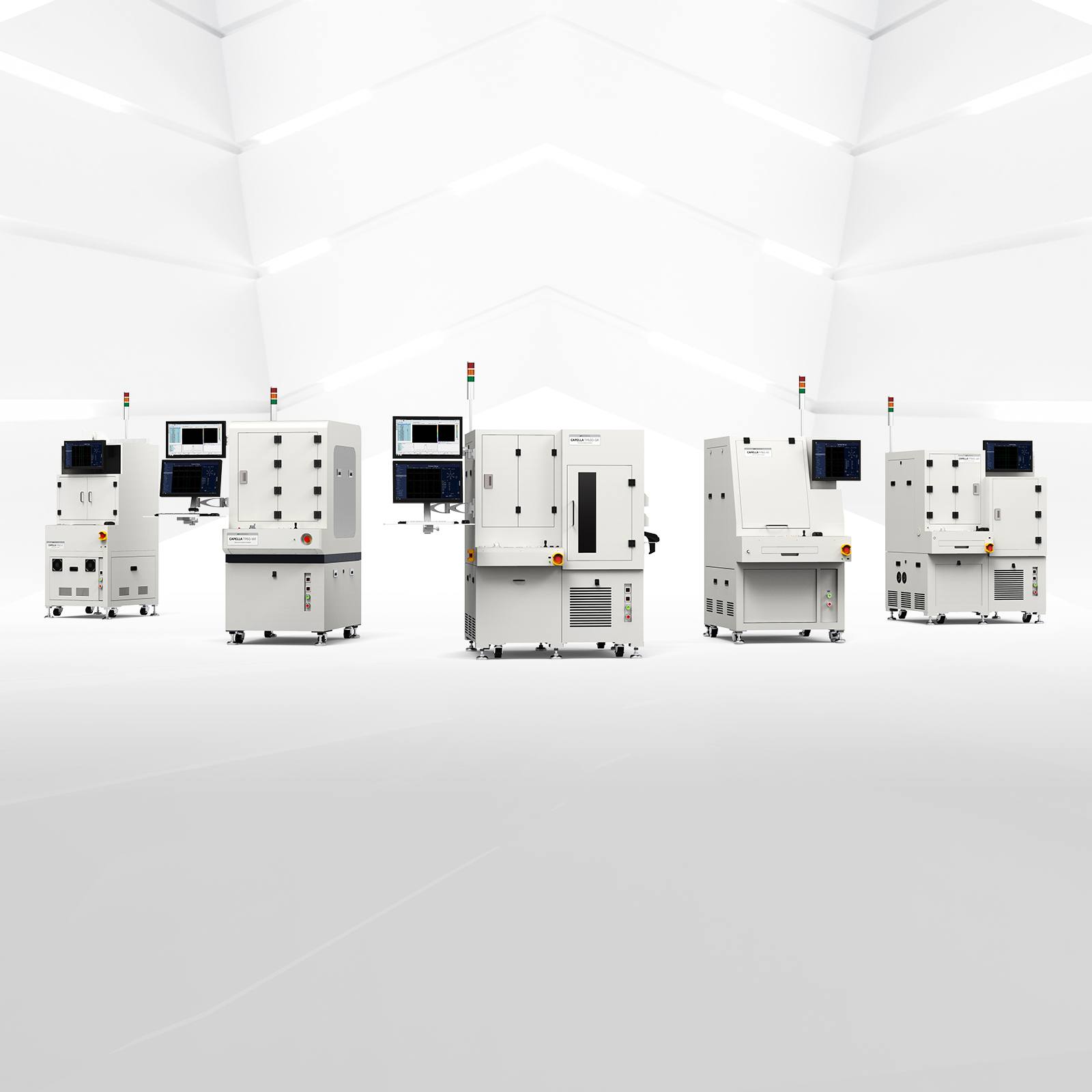
CAPELLA : Our most versatile line, covering a wide range of applications (e.g. LED and Mini LED)
Choose MPI PA for photonics test solutions that match your ambitions.
Innovation continue :
With over 20 years of experience and over 10,000 systems deployed worldwide, MPI PA is at the forefront of photonics testing technology.
Clarity and simplicity :
A nomenclature system to quickly identify the key characteristics of each product, simplifying your selection process,
Optimized support :
Discover SIRIUS, the probe control system redesigned for an optimal user experience, comparable to a personal assistant for your tests.
Flexibility and customization :
We adapt to your specific needs, offering tailor-made solutions for your business.
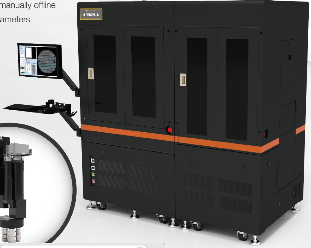
High-performance testing for VCSEL, EEL, PD, LED, OLED, micro and mini LED devices providing high-throughput testing for key device characteristics, including LIV scan curve, far field and Near Field.
Optical flexibility
Advanced control with MPI Prober Control
Hot and cold tests
Supports a wide temperature range for testing wafers, packages, and singularized chips, with the ability to handle thin/warped wafers
Precision and performance
Adaptability
Different models available to meet your specific needs, with wafer sizes up to 8 inches