Atmospheric plasma cleaning system for surface preparation: principle, advantages and applications
Are you experiencing difficulties with the quality of your substrate surfaces during soldering, wiring, thin-film deposition, hybrid assembly, etc.?
Native oxides and organic contamination on surfaces are certainly not to blame, and conventional surface preparation processes such as wet etching, fluxing or vacuum plasma treatment all have their drawbacks.
Our partner ONTOS Equipment Systems offers you an innovative, simple, effective and ultra-clean cleaning and surface activation solution: the atmospheric plasma treatment system.
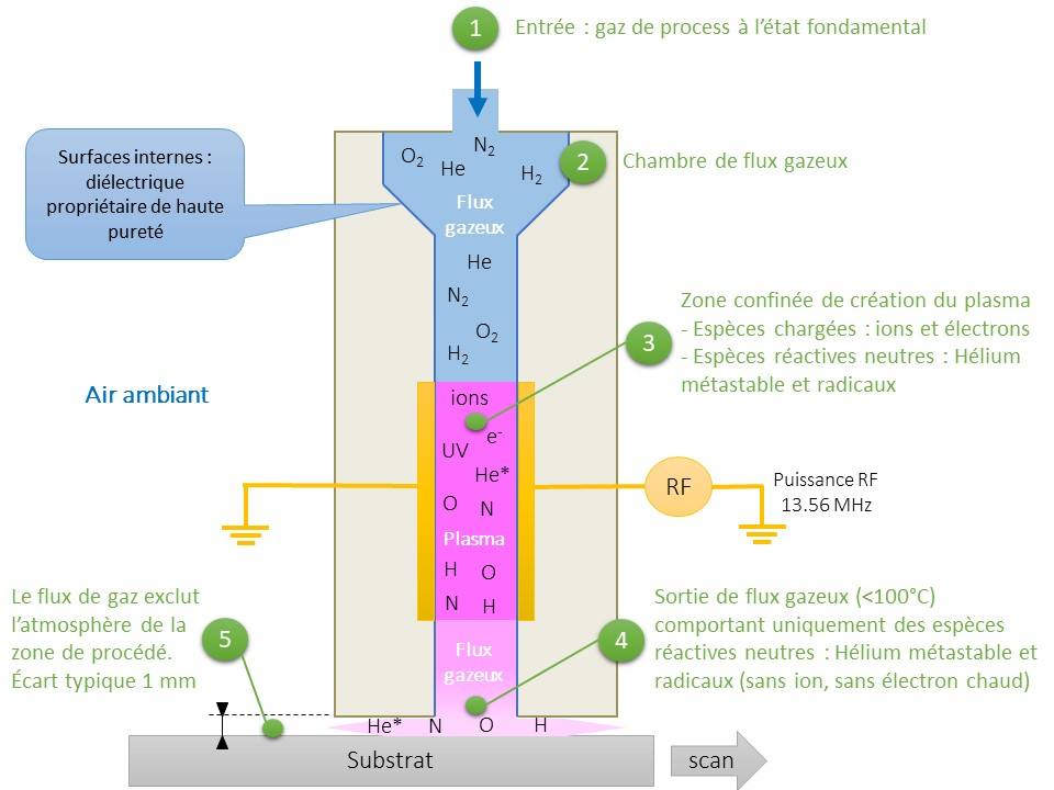
This system uses an internal glow discharge plasma ❸ which creates a high-density flow of reactive gaseous radicals ❹.
As the gas flows out of the internal plasma zone ❺, the high-energy species (ions and hot electrons) recombine within microseconds (well before coming into contact with the treated substrate surface) and the gas cools rapidly.
The carrier gas used is helium for the high quantum energy provided by the metastables. It can be replaced by argon, which is more economical, but whose metastable energy is reduced by 50%.
The stream of neutral and chemically highly reactive radicals created by the plasma reacts with the substrate surface:
It “cleans” the substrate by modifying the upper atomic layers through chemical reactions in an activated gas phase (e.g. removal of oxygen and/or carbons and hydroxyls from the substrate surface);
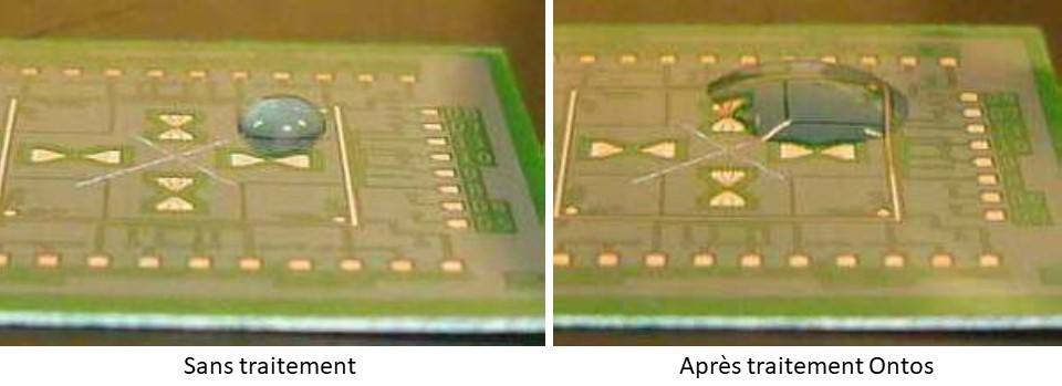
It modifies properties such as surface energy (tension), thereby increasing the adhesion and wettability of surfaces in a targeted and controlled way, making them more receptive to subsequent treatments;
It can reduce oxides and passivate metal surfaces against reoxidation for a variable period depending on the material (several hours for indium).
Cross-section of the atmospheric plasma head. Microtest diagram based on Ontos drawings.
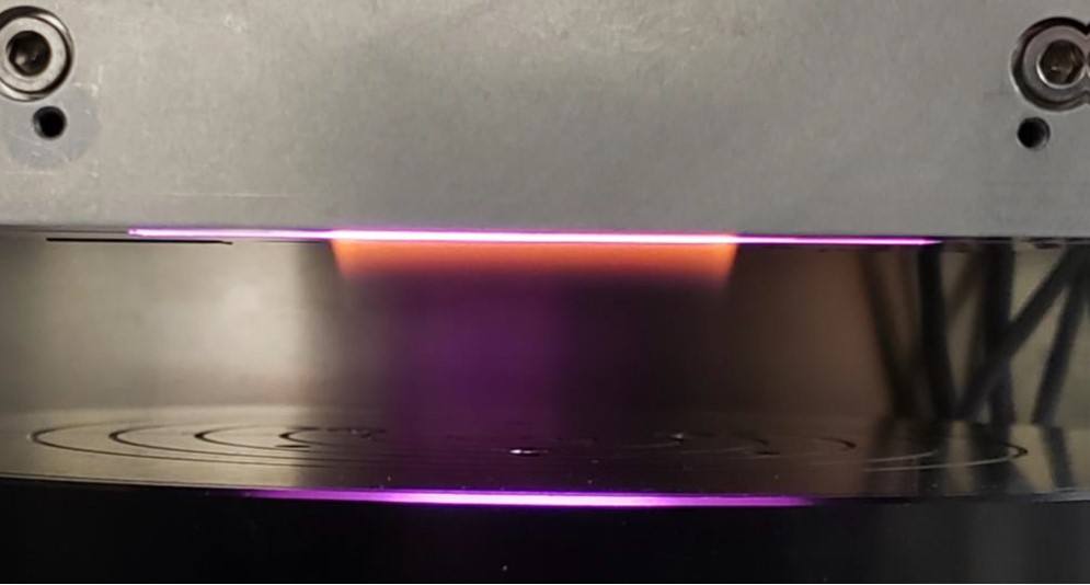
Illustration of He + N2 plasma. Ontos photo.
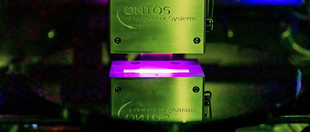
Ontos plasma head cleaning a 200mm wafer
Its advantages are numerous and differentiating:
A simple solution:
The ONTOS system eliminates the disadvantages of traditional plasma systems (no vacuum chamber requiring a relatively long pumping time, no ion bombardment and no cross-contamination, possibility of in-line processing).
An effective solution:
The process is fast (wafer processing in a few minutes), with continuous throughput capability.
It is compatible without modification with reducing or oxidizing chemistry.
It provides temporary atomic-level passivation against reoxidation of exposed metal surfaces.
An ultra-clean solution:
This dry, non-toxic process mobilizes only benign activated gases, with no by-products or waste hazardous to health and/or the environment.
There is no exposure to arc discharges, ions, bombardment, re-deposition or flaking particles.
The system is CE certified and OSHA and EPA compliant.
Some examples of surface preparation applications with the ONTOS system:
For Front-End :
Wafer cleaning
Photolithography: simultaneous removal and activation of photoresist residues
Surface activation and pre-wetting for aqueous processes
Pre-deposit preparation (cleaning and surface activation)
Surface preparation before plating.
For the Back-End :
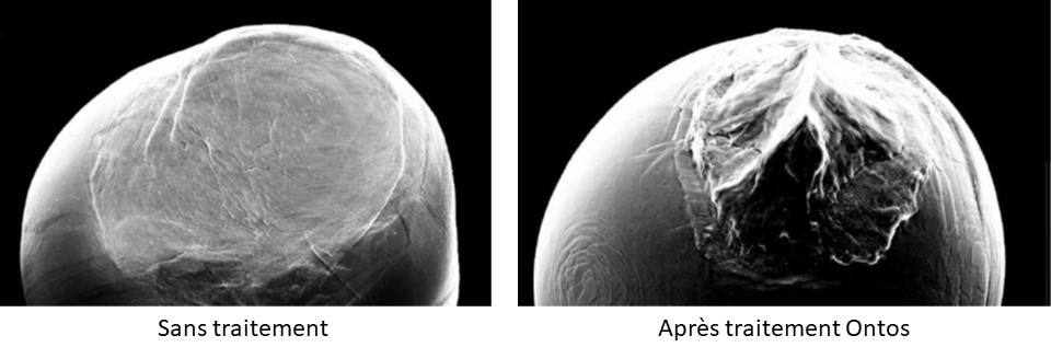
Metal-to-metal welding: surface preparation for direct interconnect bonding to remove organic matter and native under-oxides, enabling instant bonding with an ideal, highly reliable metallurgical bond.
Example of an indium-to-indium bond under identical conditions, except for surface preparation (without treatment, the oxide layer prevents indium interdiffusion). Ontos pictures
Preparation before bead cladding or direct welding
3D IC chip stacking, flip chip preparation, …
Surface activation before encapsulation
Example of surface activation on a composite material
Improved capillary filling
Direct welding of dielectrics and ohmic contacts (die-to-die, die-to-wafer, …)
Etc.
The OEM version of the ONTOS plasma head is available for integration into third-party integration into third-party, automation-compatible equipment.
Retrouvez MICROTEST et ONTOS ! 😊
Du 15 au 17 mai à la Conférence ENRIS au C2N – Centre de nanosciences et de nanotechnologies | Paris Saclay
Les 7 et 8 juin lors du dixième MiNaPAD* Conférences & Forum au WTC à Grenoble (+ajout lien sur le site)
(*) MiNaPAD = Micro/Nano-Electronics Packaging and Assembly, Design and Manufacturing Forum.